
About Pcb Thermal Relief Calculator (Formula)
In the world of electronics, effective thermal management is crucial for the longevity and performance of printed circuit boards (PCBs). A PCB Thermal Relief Calculator is an essential tool for engineers and designers, allowing them to determine the appropriate thermal relief width for surface mount technology (SMT) pads. This calculation is vital for ensuring that heat generated during operation is adequately dissipated, preventing overheating and potential failure of electronic components.
Formula
The formula for calculating PCB thermal relief width is:
PCB Thermal Relief Width = (Overall Length of SMT Pad * 0.60) / Quantity of Thermal Connecting Traces
Where:
- Overall Length of SMT Pad is the length of the surface mount pad.
- Quantity of Thermal Connecting Traces is the number of traces connected to the thermal pad.
How to Use
- Measure the Overall Length of the SMT Pad: Start by measuring the length of the SMT pad in millimeters (mm).
- Determine the Quantity of Thermal Connecting Traces: Count the number of thermal traces that connect to the pad.
- Input the Values into the Formula: Substitute the measured length of the SMT pad and the number of thermal connecting traces into the formula.
- Calculate the Thermal Relief Width: Perform the calculation to find the appropriate thermal relief width required for optimal thermal performance.
Example
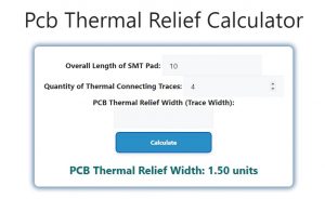
Let’s say you have an SMT pad with an overall length of 10 mm, and there are 4 thermal connecting traces.
- Overall Length of SMT Pad = 10 mm
- Quantity of Thermal Connecting Traces = 4
- PCB Thermal Relief Width = (10 mm * 0.60) / 4 = 6 mm / 4 = 1.5 mm
In this example, the required thermal relief width is 1.5 mm.
FAQs
- What is PCB thermal relief?
PCB thermal relief refers to the design technique used to manage heat dissipation from components to the PCB substrate. - Why is thermal relief important in PCBs?
Thermal relief helps prevent overheating, ensuring that components function correctly and prolonging their lifespan. - What happens if the thermal relief width is too small?
A small thermal relief width can lead to inadequate heat dissipation, potentially causing component failure or reduced performance. - Can I use this calculator for different types of pads?
Yes, this calculator can be used for various SMT pads, but ensure that the values used are appropriate for the specific pad type. - What materials affect thermal conductivity in PCBs?
Materials such as copper, aluminum, and specific PCB substrates have varying levels of thermal conductivity that influence heat dissipation. - How can I improve thermal management on my PCB?
In addition to using thermal reliefs, you can improve thermal management by optimizing component placement, using thermal vias, and choosing suitable materials. - Is there a standard thermal relief width for all designs?
No, the thermal relief width varies based on the specific application, components used, and PCB layout. - How do I determine the overall length of my SMT pad?
Measure the length of the pad from the PCB layout or consult the component datasheet for the specified dimensions. - What tools can I use to measure SMT pads accurately?
You can use digital calipers or PCB design software that provides precise measurements of pad dimensions. - How often should I recalculate thermal relief widths?
It’s a good practice to recalculate whenever you modify the PCB design or change component specifications. - Are there guidelines for thermal relief in high-power applications?
Yes, high-power applications often require more substantial thermal reliefs and advanced thermal management strategies. - Can I use thermal vias instead of thermal reliefs?
Yes, thermal vias can be used alongside thermal reliefs to enhance heat dissipation, especially for high-density designs. - What is the best way to connect thermal traces to the ground plane?
Ensure that the thermal traces are adequately wide and short, connecting directly to the ground plane for optimal thermal performance. - How do environmental factors affect PCB thermal performance?
Ambient temperature, airflow, and surrounding components can influence the overall thermal performance of a PCB. - What are the consequences of neglecting thermal management in PCB design?
Neglecting thermal management can lead to overheating, decreased performance, and premature failure of electronic components. - Is it possible to simulate thermal performance before manufacturing?
Yes, thermal simulation tools are available that can help predict thermal behavior based on your PCB design. - How does the design layout impact thermal relief efficiency?
A well-optimized layout can enhance heat flow and reduce hotspots, making thermal reliefs more effective. - What role does trace width play in thermal management?
Wider traces can carry more current and dissipate heat more efficiently, contributing to better thermal management. - How can I verify if my thermal relief design is effective?
You can verify the effectiveness through thermal imaging after the PCB is assembled and under operational conditions. - Are there industry standards for thermal relief design?
Yes, various industry standards exist that provide guidelines for thermal management in PCB designs, including IPC standards.
Conclusion
The PCB Thermal Relief Calculator is a vital resource for anyone involved in electronic design and manufacturing. By accurately calculating the thermal relief width needed for SMT pads, engineers can ensure that their PCBs effectively manage heat, leading to better performance and increased reliability of electronic devices. Proper thermal management not only enhances component longevity but also contributes to the overall success of electronic projects.